Translate

Monday 1 April 2013

Running at 200MSPS


200 MSPS working now

I'm finally sampling at 200 MSPS. for some reason I'm an expert to misunderstand datasheet.
This morning... I read carefully the ADC's datasheet and I wrote correct UCF file for my Xilinx device.
look by yourself:

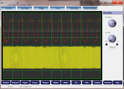
10 MHz square wave

The waveform compared with the same inoput signal published in my previous post looks much more like a square wave, obviously as I can only have the first 3 harmonics... it can't get better than that, even if I increase the input bandwidth. Therefore I'm really satisfied. 


Next:
1) assemble and test channel 2
2) finish to design the USB isolation module (I don't want to damaged my PC)
3) to complete the SW!

Sunday 31 March 2013

FFT and Spectrum Analyzer

How to use an oscilloscope as Spectrum analyzer...

I start to love my oscilloscope. I honestly can't say I have used something that works so well.
I have just finished to add the FFT functionality... and I was amazed with the results, accuracy and speed!
I'm sampling only @100MSPS , 2K buffer. 

1 MHz Sine wave

By applying 1 MHz sinewave, as you can see the spectrum analyzer is correctly indication 1 MHz. The smae indication you can get with the time cursor, but is not so funny with it. 


 after I have applied 1 MHz, I have then applied 2 MHz, 3MHz, and so  up to 40 MHz.
and the spectrum analyzer always gives the correct results:

2MHz sine wave


4 MHz sine wave


 10 MHz Sine wave


20 MHz Sine 


30 MHz sine


Square wave!

The square wave is the most interesting to watch from a spectrum point of view. As you probably know the square wave has got only odd harmonics, e.g. the 1st, 3rd , 5th etc.
Let see the spectrum on a 1 MHz and a 10 MHz square wave:

1 MHz Squarewave

As you can see, the spectrum analyzer correctly report the 1st, 3rf, 5th, 7th, etc. 


10 MHz Square-wave

a 10 MHz square-wave, and we can still see  all the odd harmonics! the Oscilloscope works very well!


 100 KHz Square-wave

100 KHz the spectrum analyzer still works OK, but the resolution is poor. the is due to the fact that with 2048 bytes of buffer, the minimum resolution I can get by sampling at 100 MHz is 100MHz/2048 = 48.8 KHz (approx)... so I was thinking that in the next prototype I will probably add more ram.... maybe changing the FPGA or adding extra ram on the board..


Friday 29 March 2013

Vertical and Horizontal cursors

Adding more functionality on the Oscilloscope

Horizontal and vertical cursors

Designing a digital oscilloscope that is actually useful for a designer seems to be an hard task today for many company. Probably one reason is that the person who write the specs... most of the time.... is not a designer... It could be a very clever chap but sometime  doesn't use the oscilloscope very often.
For example one of the most useful function on a modern oscilloscope is to be able  to make horizontal and vertical measurement. Now while most oscilloscope have this functionality, a functionality very useful is to bring an horizontal cursor back to the screen, without the need to turn 100 times the knob, or without the need to zoom out, then bring the cursor in the middle, then zoom in, and so on.
I have added a simple button that does that for me! 
In many oscilloscope, for some reason the cursors interface is quite a mess, you need to press a button to switch between he cursor and when you press one more time you need to do again and again...
why make the life difficult?
see the GUI below and you immediately understand how it works.


Se you at next time.


Thursday 28 March 2013

AN oscilloscope that I would use in the lab

Getting better and better

The Oscilloscope it start to be good enough to bring it in the lab with me.
On the screen the user has all the information he needs.
I have slightly changed the look as well. 
I'm so happy to have started this project! I still can't believe I have done this!


Next time... I will:
adding the menu for Cursors, Measure, Math (with the FFT).

Tuesday 26 March 2013

a working USB Occilloscope

The oscilloscope SW is very fast!

Last week end I finally found  a working solution for the interpolation algorithmic and tonight I decided to work on the SW side to make the SW very responsive. I'm very impressed how the GUI react with the commands considering the amount of work is doing to calculate the interpolation of a waveform.
I'm also impressed with the linearity displayed from the sinc(x) exp(-x^2/3) algorithm.
So now my task for the next day is to assemble the second channel on the PCB and to finish the SW.


Sunday 24 March 2013

The Oscilloscope is growing up

More waveform

I made a bit more work on the interpolation algorithm, I haven't finished yet... but for the time being I will stop for now to work on the interpolation algorithm as I have achieved some good result today.
So the Oscilloscope is still sampling only at 100 MHz! (200 MHz next week end I guess).
Let see some waveform:


1 MHz Sinewave

Not too bad I think... it is still possible to see some issues due to common mode noise that probably goes inside the input ( 1MHz) of the oscilloscope and is displayed, as at moment the oscilloscope is still not isolated from the PC I must leave with it until I isolate it.


 1 MHz squarewave

Not too bad I think, considering that the square wave is the function with lots of  harmonics   .


5 MHz sine wave 

not too bad I think


5 MHz square wave

Not too bad considering I'm sampling at 100 MHz!


10 MHz sine wave

pretty good!


10 MHz square wave

Not too bad  considering that the input is a 10 MHz square wave and I've got only 10 samples to rebuilds.
I wish to thanks all the person  that are following this blog  for the excellent suggestions on how to design the interpolation algorithm. When you buy an oscilloscope and you read sinc(x) interpolation. Don't believe it  without a good windowing you have overshoot all over the place. in my case I'm using a sin(x)e(-x^2/3) interpolation, the Gaussian works pretty well in reducing the overshoot. 


What to do now?

1) improve the SW

2) finish to design the isolator ( the noise should further reduce)

3) sample at 200 MSPS ( so far I haven't done because of a mistake of mine in choosing the clock pin of the FPGA)


Saturday 23 March 2013

Still problems on the interpolation

I love DSP but I'm bad at it!


It looks like I'm a bad SW designer... 
I'm still not sure I understood how to interpolate a raw data from the FPGA buffer to the screen.
In the picture below I have in yellow the raw data from the FPGA, and in red the interpolated data using the sinc(x) algorithm.
Now how you can see, there is nothing that suggest why I should have all that ringing.


In order to show the problem even better I have zoomed the image(see below): in red I still have the interpolated data, while in yellow I have the raw data.
From the raw data, I can see some small ringing that for some reason get amplified in red when I interpolate .
For example if you look at that negative edge... it doesn't look right isn't it? 


the above GUI is written using Lazarus . The function that create the interpolated data is :


function sinc_interpolation(buff: TCH_BUFF; Fsample: float; t: float): float;
var
  i: integer;
  sum: float = 0;
  x_nt: float;
  Ts: float = 0;

begin

 {
  x(t) = sum [ Xn sinc(pi/T(t-nT))] sum all the n...
  }

  Ts := 1 / FSample;  // sample time
  sum := 0;
  for i := 1 to BUF_SIZE - 2 do // remember to fix the bug inside the FPGA
  begin
    x_nt := buff[i] * sinc((t - i * Ts) / Ts);
    sum := sum + x_nt;
  end;
  Result := Sum;

end;  
When I call that function I set:
 Fsample = 100000000.0; (100 MHz)
t = time I want to diplay on the screen ( I start to calculate t  starting from the middle of the buffer)
and buff is the buffer from the FPGA

Do you think the code  above is correct?
any comment is welcome.


Tuesday 12 March 2013

improving the sinc(x) interpolation

I need to improve the interpolation algorithm

I'm working on the sinc(x)/x algorithm... and I'm having some trouble understanding some effect I can see on the scope.
in the picture below I'm displaying on CH1 the interpolated signal, while on CH2 I'm displaying the FPGA buffer

the first  picture is is a sinewave 1 MHz  as you can see the sinewave is a bit wobbly...  the problem is that if I use a linear interpolation to display CH1... then it looks not too bad ( see old post)


The wobbly effect is more evident when I use a triangle wave... as you can see... I do have some problem...
now I'm running out of idea... any suggestion is really welcome!


Sunday 10 March 2013

Oscilloscope specifications


Oscilloscope DSO-2-200-B


Characteristics


Characteristics
DSO-2-200-B
Bandwidth
20 MHz
Channels
2
Sample Rate on Each channel
200 MS/s
Record Length
3K points at all time base on all mode
Vertical resolution
8
Vertical sensitivity
5mV/div to 5 V/div on all modes
DC Vertical accuracy
3.00%
Vertical Zoom
Vertically expand or compress a live or stopped waveform
Maximum input voltage
100 Vrms derated at 20 dB/decade above 50 Khz
Position range
5mV to 500 mV/div (1:1 probe)
50 mV to 5V/div (1:10 probe)
Input coupling
AC, DC
Input impedence
1 Mohm, in parallel with 20pF
Time Base Range
20 ns to 5 s/div
TimeBase accuracy
50 ppm
Horizontal Zoom
Horizontally expand or compress a live or stopped waveform


Acquisition mode


Mode
Description
Peak Detect
Capture Glitches as narrow as 30 ns at all base setting
Sample
Raw data
Average
Waveform avareged, selectable 4,16
Single sequence
To capture a single event
Roll
At acquisition time > 100 ms/div


Trigger Types

Trigger
Description
Edge (rising, falling)
Positive or negative slope on any channel, coupling selection AC, DC
Pulse width
Trigger on a pulse width less than, greater than, equal to, or not equal to, a selectable time limit from 30 ns to 1 sec


Trigger source

CH1, CH2


Cursors


Characteristic
Description
Types
Amplitude, Time
Measurement
t1-t2,Freq, V1-V2


Automatic waveform measurement

+Width, -Width, Rise time, Fall time, Max, Min, Peak-Peak, RMS


Waveform Math

Characteristic
Description
Operators
+ , - , * , FFT
FFT
Hanning, 2048 sample points
Sources
CH1, CH2 of any combination above


Connection to a PC

Characteristic
Description
Connection to a PC
USB. Default, option Ethernet
OS supported
Windows7, Windows8


10 MHz Input square wave

Time to play!

I'm still sampling at 100 MHz! the input signal is a 10 MHz square wave.
CH1 shows the actual square wave, while CH2 at moment shows the FPGA raw buffer.
I'm using the sinc(x) interpolation to rebuild the original wave form, and I've learnt 2 things.
1. From a spectrum point of view the beginning of the raw data is seen as a step  gradient, which goes against the hypothesis of  the Shannon theorem. That explain the first "distortion" of the CH1. 
So it's easy to fix.
2. Now the second point is that the square wave is a little wavelike on the top  and bottom... that I guess is because I haven't fixed the problem of the floor noise completely yet!
Therefore I'm going to work on that now.
1. by fixing the noise floor I think the square wave will look even better.
2. I could further improve the waveform by play with the delay in the DLL, so I could create an equivalent sample of 1 GSPS  and therefore the waveform should look very squared. ( Now I understand why so many USB oscilloscope use the ETS)


Any suggestion is welcome. 

First experiment with the sinc(x) interpolation


Sinc(x) interpolation

The Shannon Theorem states that given a signal  limited in bandwidth with the maximum harmonic fc <= 1/2 Fsample you can rebuild the original signal by interpolating :

x(t) = \sum_{n=-\infty}^{\infty} x[n] \cdot {\rm sinc}\left(\frac{t - nT}{T}\right)\,


I am applying on CH1 and CH2 a constant signal, and I'm plotting CH2 with a linear interpolation and CH1 with a Sinc(x) interpolation... unfortunately it looks like I'm a bad DSP designer as CH1 is the sinc itself! :-)
I wanted to write it  down because I found the CH1 waveform funny.  Its actually pretty!
So... last week I made lot's of progress, I'm now sampling at 100 MSPS... on the above picture the horizontal resolution is 20 nsec/div...
I will post again once I fixed the sinc(x) problem!

Monday 4 March 2013

Another little step

Getting better

Yesterday night  I promised myself to work on the SW side as I knew the noise issue was easy to fix... But as hardware engineer I wanted to fix it.
As you can see, the Oscilloscope it start to be useful! The next 2 pictures are showing a sine wave and a square wave of 2.31 Vpp , 500 KHz. Please notice that the X, Y scale is still not working!


Sunday 3 March 2013

The first waveform

It start to work!!

This is my first waveform! the X and Y scaling are still not working...
I am applying an input signal of only  280 mVpp, 50 KHz sine wave .  How you can see below at moment the scope has a floor noise of 4 - 5 mV which I believe I can fix.
The noise floor is due to the FTDI chip .
Unfortunately the FTDI USB chip (at moment) is not isolated from my Scope, and this seems causing some noise issues. My plan is to insert a galvanic insulation between the scope and the FTDI, and I guess the Noise floor should improve.


My plan for next week:
work on the SW side only, so the scope start to behave like a proper scope.
maybe (if I've got time ) solder the channel 2 .

Friday 1 March 2013

API building

I started designing the API to communicate with the oscilloscope

When I run the SW and you press the connect button the SW check how many oscilloscopes are connected if more than one, then you need to select one. So... in theory you can connect as many oscilloscope you want on a PC.
then check for the Device ID and the revision. it depend from the device ID, the behavior of the SW will be different.
I can now control the AC/DC  coupling, and control the overall GAIN and attenuation of the input stage amplifier!
See you soon!

Tuesday 26 February 2013

I have tested the input stage (with the exceptions of the 2 relays). I'm using as signal generator an HP 8116A, (50 MHz sin,saw,square)... the frequency response is quite flat, and I can compensate the input stage with the input compensation network I designed.
I'm using an old Tektronix 2205-40 as oscilloscope... not the best this days... but good enough for the job.

I have also finished to design the FPGA (for the time being) and in the next few days I need to go back on the SW side and design the API to communicate (from my SW) with the FPGA.
To do this I'm using a FTDI chip that is delivered with a *.dll that simplify the design of the API!

Keep watching the next few days this blog! I bet at the end of the week I will be able to see some waveforms from my GUI.


Thursday 21 February 2013

Oscilloscope assembly part2 + FPGA JTAG

I have almost finished to assemble channel 1 of the oscilloscope.
so far everything seems working!

I connected the Xilinx's USB programmer to the JTAG chain of the FPGA ad Impact sees the FPGA:
That is a very good news! I can now program the FPGA and start doing basic testing like switch the AC DC relays...control the attenuation, gain, etc.
I'm still waiting an op amp from RS which is supposed arrive tomorrow.
if everything goes well, next weekend I should be able to start to test the input amp. stage!

Wednesday 20 February 2013

Start to build the Oscilloscope + FPGA block diagram

I started to build the oscilloscope. I tested the 3V analog, the 1.2V digital, the 3.3V digital. and they seems OK. I'm waiting some components, tomorrow I should be able to test the -5V and check the susceptibility on the 5V analog as well. Each amplification stage can be powered individually, so if there is a fault on the board it should be easily fixed. I believe in the next 2 days I should manage to assemble the board.


It would be nice to be so proficient at  work, unfortunately I'm tagged as "digital" designer and I can only do 30% of what I could...I get very frustrated for that... well... life is too short to get too upset I guess...


FPGA Block diagram


The above is the FPGA block diagram. The FPGA has got an UART to communicate externally with an FTDI chip or a wiznet. the RX_UART (uups I wrote TX_UART above) send the received data to the interpreter which decode the input and drive the trigger unit, the AC_DC relay or the attenuator.
on the TX side the trigger unit gets the CH1, CH2 data, and accordingly to the command received from the INTERPRETER trigger CH1 or CH2. data are then send to a module that I call TX_CPU, and finally sent to the UART_TX.


THE PCB has just arrived


The PCB has just arrived.
I'm starting populating the PCB next week end. Tonight I want to finish to design the FPGA which is almost done.
the PCB fits perfectly in the metallic box

The box also looks quite pretty.


Monday 18 February 2013

FPGA for the Digital Oscilloscope


FPGA

The oscilloscope has a Xilinx FPGA  Spartan-3AN-50-TQ144. I have chose this FPGA for 2 reasons:
  1.  it doesn't need an external Flash memory, making therefore the assembly slightly easy.
  2. the package
the negative side of the FPGA are:
  1. quite small ( I can't ecpect complex triggering functionality)
  2. I can have only 2Kbyte of buffer for each channel. t
As I have designed FPGA for most of my career I believe I can manage to get the best from this small device. I'm using ISE Webpack 13.4. And I've just designed the UART to communicate with an FTDI chip.
Follow a list of register to communicate with the FPGA:

ADDRESSREG NAMER/WD7D6D5D4D3D2D1D0


0ID_PRODUCTR

ID_PRODUCT


1REV.R

REVISION


2CHAN_SELW


CH4CH3CH2CH1
3AC_DCW


AC/DC
4ATTNW


ATTN2ATTN1ATTN0
5TRIG_ARMW


FORCENORMAUTO
6TRIG_TYPEW


FALLINGRISING
7TRIG_AMPLITUDEW


8TRIG_OPTIONW


9DATA_READYR


On the next post I will show the Oscilloscope block diagram.

Saturday 16 February 2013

Yet Another Digital Oscilloscope

I discovered to love electronics from at the age of 12 when I started read my daddy's book "how to build your own radio".  
After that book I read another one and then another and another and so on...Today I'm one of the few lucky guys that get payed for something that would probably do for free. I design electronics ... but unfortunately at  work I don't decide what to design... so one day I said..."why don't start to design something for fun?"
What about an Oscilloscope?

Designing a good oscilloscope is challenging...this will be my first real attempt to do it. As I am aware of the challenge I decided to design a low specs. If the experiment will be successful I will design an higher specs in the future.

Let's start with some basic specifications:

  1. Analog Bandwidth, DC- 60 MHz with 1% max ripple or better
  2.  +-20V max input signal
  3. USB/Ethernet connected
  4.  trigger AUTO, NORMAL, (rising, falling)
  5. 4 Kbyte buffer
  6. 2 channels

A few months later...

YES the PCB is done! I have used DesignSpark from RS. I think is probably the best free CAD around.


I have placed the order on www.pcbtrain.co.uk I have used them in the past and I think they are quite good!
The PCB costed me around 115£ for one in 15 working day...
While waiting the PCB coming I started designing the  GUI interface.
What tool to use? I wanted the GUI to work on Windows and Linux...
I have found Lazarus from http://www.lazarus.freepascal.org/ if you have used Delphi in the past you shouldn't found any problem using it. it looks like the old interface of Delphi.

After 2 weeks of work mostly in the weekend and in the evening after work I managed to have that:


Not too bad... for a home project...
In the next blogs I will explain more in details the project....